Silicon carbide (SiC) or gallium nitride (GaN) switching operations are limited by the busbar stray inductance because the inductance is present in the commutation loop. It’s through the commutation path that current travels through the dc bus capacitor, the switching devices, and the busbar or printed circuit board (PCB) connecting them.
In this article, we’ll first review what stray inductance does to an electric vehicle (EV) power electronic circuit. Then, we’ll take the busbar and PCB geometry into account for controlling it with SiC and GaN examples.
Consider a 600-Vdc bus switching a 10 A load, which is a standard test case for evaluating commutation loop design. Every time the switch turns off, the drain-source voltage overshoots the bus voltage, and the size of the overshoot depends on the loop inductance and the rate of current change during switching.
The difference between those two loop inductances shows up directly in Figure 1, which plots the same switching event at 10 and 40 nH. Here, only the loop inductance changes between the two cases.
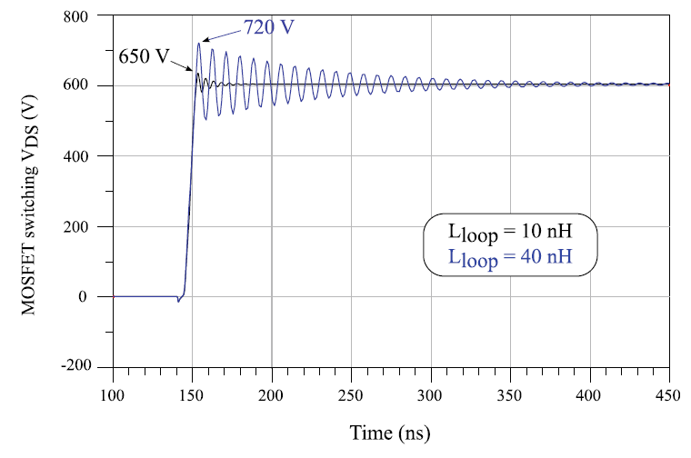
Figure 1. Drain-source voltage overshoot for the same switching event at 10 nH and 40 nH loop inductance. (Image: International Journal of Energy Research)
At 10 nH, the switch-off event overshoots the 600 V bus by 50 V, which leads to a peak of 650 V. At 40 nH, a typical value for TO-247 packages, the overshoot more than doubles to 120 V, reaching 720 V. Every other circuit parameter is kept constant in these cases.
How does busbar geometry control loop inductance?
Because loop inductance comes from the physical geometry of the current path, modifying that geometry is a direct way to reduce stray inductance. The key is how the current’s outbound and return paths sit relative to each other inside the busbar or PCB stack. When we run them side by side in the same layer in the form of a lateral loop, their magnetic fields add up.
However, there is an alternate way to address the problem. Figure 2 illustrates a vertical loop that stacks the go and return paths directly on each other.

Figure 2. PCB commutation loop with outbound and return current stacked on facing layers to cancel magnetic flux. (Image: Energies)
In this configuration, the GaN devices and the dc bus capacitor sit on the top layer, with the return path on the layer directly beneath, connected by vias. Current in the top layer flows in one direction, and current in the layer below flows in the opposite direction.
This phenomenon cancels their magnetic flux to a large extent. A lateral loop does not allow this type of magnetic flux cancellation because the geometry does not permit it.
How do engineers cut busbar inductance in SiC converters?
The same flux-cancellation principle extends beyond PCB loops to busbar design for discrete SiC packages. Let us follow one busbar optimization study through eight commutation loop layouts for a TO-247 device pair, each simulated with Ansys Q3D.
The full progression appears in Table 1, which tracks loop inductance from a baseline layout to the final layout tested.

Table 1. Commutation loop inductance across eight TO-247 busbar layout iterations, from baseline to final design. (Image: Electronics)
The baseline layout is a straightforward device mounting with no optimization, and it measured 26.3 nH. By repositioning decoupling capacitors directly between the devices (Layout-2 and Layout-5), the loop inductance drops to 19.7 nH as mutual flux cancellation increases. Adding a dedicated four-layer decoupling capacitor card (Layout-7) further reduces inductance to 18.0 nH.
In the final result, the card is edge-plated so that its leads solder as close to the device as possible, resulting in the lowest possible inductance of 16.7 nH. It’s a 36% reduction in inductance from the baseline.
How can GaN PCB layout reduce loop inductance?
This same loop-geometry principle scales even further once the entire commutation loop is embedded directly inside the PCB itself. Testing was carried out on a GaN half-bridge inverter leg across three PCB integration levels, ordered by how tightly the loop is packed into the board.
Table 2 compares the stray inductance of the power loop across the three layouts at 1, 10, and 100 MHz.

Table 2. Stray inductance in the power loop at 1 MHz, 10 MHz, and 100 MHz across 2D, 2.5D, and 3D chip-on-chip PCB integration of a GaN half-bridge leg. (Image: Energies)
A planar 2D layout, with the two GaN devices mounted side by side, measures 8.9 nH at 1 MHz. A 2.5D layout, mirroring one device on the top of the board and the other on the bottom, brings that down to 7.56 nH. The full 3D layout embeds the decoupling capacitors vertically inside the PCB alongside the mirrored devices and reaches 1.93 nH.
The same ranking holds up to 100 MHz, the highest frequency tested. The 3D layout still measures under 2 nH there, while the 2D and 2.5D layouts fluctuate.
The SiC example needed eight layout iterations for a one-third reduction. This GaN result comes from restructuring the PCB itself, and it goes further. A shielding technique built into the busbar planes on the same hardware also cuts common-mode emission at the inverter input by more than 17 dB.
Summary
When designing a commutation loop for a SiC or GaN converter, loop inductance needs to be properly accounted for. Start by checking how much overshoot your own loop inductance adds at your actual rate of current change, similar to the difference between the 50 and 120 V overshoot cases. Then, look at the current path geometry before you reach for snubbers or a slower gate drive.
Stacking current paths on facing PCB layers, repositioning the decoupling capacitor, and embedding the loop inside the board have each delivered measured reductions. Those range from about a one-third cut on SiC hardware to a fivefold cut on GaN PCBs.
References
- The role of power device technology in the electric vehicle powertrain, International Journal of Energy Research
- Power Converters Using S-Parameters and EM Simulations, Energies
- GaN Power Transistors in Converter Design Techniques, Energies
- Busbar Design for High-Power SiC Converters, Electronics
EEWorld Online related content
- How to shrink size and boost performance with low inductance electrolytic capacitors
- How do snubber circuits offer circuit protection in power electronics?
- What are the challenges of designing high-frequency PCBs for EVs?
- How do parasitic inductances affect switching performance?
- Parasitic capacitance, inductance, and displacement current
- Optimizing discrete SiC devices
Filed Under: FAQs, Featured Contributions, Power Electronics